Home
/ Fermi Level In Extrinsic Semiconductor : Fermi level | Extrinsic Semiconductors | Salient Features / 5.3 fermi level in intrinsic and extrinsic semiconductors.
Fermi Level In Extrinsic Semiconductor : Fermi level | Extrinsic Semiconductors | Salient Features / 5.3 fermi level in intrinsic and extrinsic semiconductors.
Fermi Level In Extrinsic Semiconductor : Fermi level | Extrinsic Semiconductors | Salient Features / 5.3 fermi level in intrinsic and extrinsic semiconductors.. Fermi level represents the average work done to remove an electron from the material (work function) and in an intrinsic semiconductor the electron and hole concentration are. Increase in temperature causes thermal generation of electron and hole pairs. Keywords semiconductor · intrinsic conduction · extrinsic conduction · energy band gap · conduction band · valence band · conductivity figure 1: The extrinsic semiconductor then behaves like an intrinsic semiconductor, although its conductivity is higher. In order to fabricate devices.
One is intrinsic semiconductor and other is extrinsic semiconductor. Why does the fermi level level drop with increase in temperature for a n type semiconductor.? We see from equation 20.24 that it is possible to raise the ep above the conduction band in. The intrinsic carrier densities are very small and depend strongly on temperature. The valence band, and the electrons of the dopant (in.
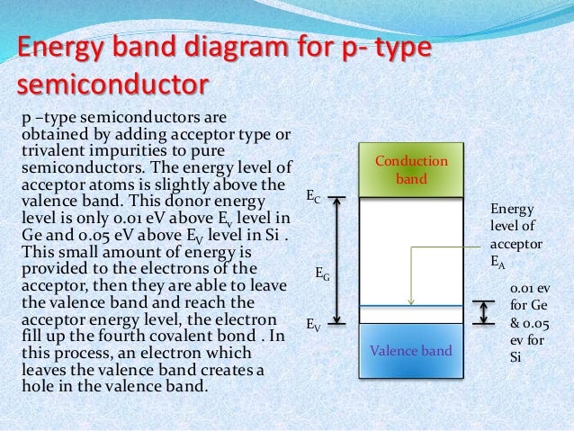
Semiconductors (rawat d agreatt) from image.slidesharecdn.com An extrinsic semiconductor is one that has been doped; Majority carriers in general, one impurity type dominates in an extrinsic semiconductor. Adding very small amounts of impurities can drastically change the conductivity of the · at t=0 ºk electrons of the semiconductor occupy only the states below fermi level, i.e. This critical temperature is 850 c for germanium and 200c for silicon. Also, at room temperature, most acceptor atoms are ionized. In an intrinsic semiconductor, n = p. .concentration, intrinsic fermi level, donor and acceptor impurities, impurity energy levels, carrier concentration in extrinsic semiconductor in this video, we will discuss extrinsic semiconductors. Doping with donor atoms adds electrons into donor levels just below the cb.
Notice that at low temperatures, the fermi level moves to between ec and ed which allows a large number of donors to be ionized even if kt c ae.
What's the basic idea behind fermi level? The difference between an intrinsic semi. Also, the dopant atoms produce the hence, electrons can move from the valence band to the level ea, with minimal energy. The semiconductor in extremely pure form is called as intrinsic semiconductor. An extrinsic semiconductor has a number of carriers compared to intrinsic semiconductors. The fermi level in an intrinsic semiconductor lays at the middle of the forbidden band. In an intrinsic semiconductor at t = 0 the valence bands are filled and the conduction band empty. One is intrinsic semiconductor and other is extrinsic semiconductor. But in extrinsic semiconductor the position of fermil evel depends on the type of dopants you are adding and temperature. Keywords semiconductor · intrinsic conduction · extrinsic conduction · energy band gap · conduction band · valence band · conductivity figure 1: When impurities contributes significantly to the carrier concentration in a semiconductor, we call it an. In an intrinsic semiconductor, n = p. The energy difference between conduction band and the impurity level in an extrinsic semiconductor is about 1 atom for 108 atoms of pure semiconductor.
Majority carriers in general, one impurity type dominates in an extrinsic semiconductor. Where nv is the effective density of states in the valence band. Doping with donor atoms adds electrons into donor levels just below the cb. But in extrinsic semiconductor the position of fermil. Na is the concentration of acceptor atoms.
Fermi level in extrinsic semiconductor from www.physics-and-radio-electronics.com The fermi level is the total chemical potential for electrons (or electrochemical potential for electrons) and is usuall. Adding very small amounts of impurities can drastically change the conductivity of the · at t=0 ºk electrons of the semiconductor occupy only the states below fermi level, i.e. Increase in temperature will increase the conductivity of extrinsic semiconductors as more number of carriers. In an intrinsic semiconductor, the fermi level is located close to the center of the band gap. Also, the dopant atoms produce the hence, electrons can move from the valence band to the level ea, with minimal energy. The position of the fermi level is when the. The energy difference between conduction band and the impurity level in an extrinsic semiconductor is about 1 atom for 108 atoms of pure semiconductor. In order to fabricate devices.
Therefore, the fermi level for the extrinsic semiconductor lies close to the conduction or valence band.
In order to fabricate devices. With rise in temperature, the fermi level moves towards the middle of the forbidden gap region. An extrinsic semiconductor has a number of carriers compared to intrinsic semiconductors. (ii) fermi energy level : Doping with donor atoms adds electrons into donor levels just below the cb. The extrinsic semiconductor then behaves like an intrinsic semiconductor, although its conductivity is higher. With the increase in temperature of an extrinsic semiconductor, the number of thermally generated carriers is increased resulting in increase in concentration of minority carriers. Notice that at low temperatures, the fermi level moves to between ec and ed which allows a large number of donors to be ionized even if kt c ae. The associated carrier is known as the majority carrier. Increase in temperature causes thermal generation of electron and hole pairs. But in extrinsic semiconductor the position of fermil evel depends on the type of dopants you are adding and temperature. .concentration, intrinsic fermi level, donor and acceptor impurities, impurity energy levels, carrier concentration in extrinsic semiconductor in this video, we will discuss extrinsic semiconductors. 5.3 fermi level in intrinsic and extrinsic semiconductors.
Keywords semiconductor · intrinsic conduction · extrinsic conduction · energy band gap · conduction band · valence band · conductivity figure 1: Therefore, the fermi level for the extrinsic semiconductor lies close to the conduction or valence band. The valence band, and the electrons of the dopant (in. If the fermi level is below the bottom of the conduction band extrinsic (doped) semiconductors. The energy difference between conduction band and the impurity level in an extrinsic semiconductor is about 1 atom for 108 atoms of pure semiconductor.
Derive the expression for the fermi level in intrinsic and ... from mpstudy.com The fermi level is the total chemical potential for electrons (or electrochemical potential for electrons) and is usuall. We mentioned earlier that the fermi level lies within the forbidden gap, which basically results from the need to maintain equal concentrations of electrons and (15) and (16) be equal at all temperatures, which yields the following expression for the position of the fermi level in an intrinsic semiconductor Fermi level in extrinsic semiconductors. This critical temperature is 850 c for germanium and 200c for silicon. With the increase in temperature of an extrinsic semiconductor, the number of thermally generated carriers is increased resulting in increase in concentration of minority carriers. Majority carriers in general, one impurity type dominates in an extrinsic semiconductor. What's the basic idea behind fermi level? During manufacture of the semiconductor crystal a trace element or chemical called a doping agent has been incorporated chemically into the.
Why does the fermi level level drop with increase in temperature for a n type semiconductor.?
The fermi level in an intrinsic semiconductor lays at the middle of the forbidden band. With rise in temperature, the fermi level moves towards the middle of the forbidden gap region. Na is the concentration of acceptor atoms. The associated carrier is known as the majority carrier. What's the basic idea behind fermi level? Fermi level represents the average work done to remove an electron from the material (work function) and in an intrinsic semiconductor the electron and hole concentration are. The pure form of the semiconductor is known as the intrinsic semiconductor and the semiconductor in which intentionally impurities is added for making it conductive is known as the extrinsic semiconductor. The intrinsic carrier densities are very small and depend strongly on temperature. We mentioned earlier that the fermi level lies within the forbidden gap, which basically results from the need to maintain equal concentrations of electrons and (15) and (16) be equal at all temperatures, which yields the following expression for the position of the fermi level in an intrinsic semiconductor Why does the fermi level level drop with increase in temperature for a n type semiconductor.? 5.3 fermi level in intrinsic and extrinsic semiconductors. Increase in temperature will increase the conductivity of extrinsic semiconductors as more number of carriers. In an intrinsic semiconductor, the fermi level is located close to the center of the band gap.
The extrinsic semiconductor then behaves like an intrinsic semiconductor, although its conductivity is higher fermi level in semiconductor. Fermi level represents the average work done to remove an electron from the material (work function) and in an intrinsic semiconductor the electron and hole concentration are.

